 Figure 1
Wilf Rigter 09/2001
This article explains the behavior of bicore circuits using the so called Shok architecture. The Shok bicore is the circuit Mark Tilden used in his Shok Walkers and the circuit was more recently presented in the ShokHead and ShokPopper designs. Here is the accompanying Theory of Operation of those circuits:
"Shok" architecture is a technique pioneered by Mark Tilden
describing controlled state changes of Bicore style circuits via chip
power or enable toggling. When a Bicore circuit is powered on, it
will resume a state opposite to what it was when it was powered off,
this effect can either be duplicated by pulsing the enable line or by
pulsing power to the chip itself. This is called "shoking" the
Bicore. The power-on state can also be pre-determined by biasing the
voltage across the Bicore capacitors. A photodiode attached directly
across the Bicore charge capacitor will pre-bias the shoked output.
The addition of tactile sensors is easily implemented by attaching a
switch from the input of the Bicore to +Vdd. When the switch is
closed, it forces that side high, presetting the state of the Bicore
on the next pulse cycle.
Probably one of the simplest photovore circuits to date, the core
circuit consists of a 6 part count and a solar-engine. Either 74AC240
or 74HCT240 will work but we recommend using the AC series for better
output drive current. The ShokPopper will not work under battery
power unless the enable line is pulsed.
Shok effect was discovered rather than designed and the Shok circuits based on this effect show such a discovery can lead to remarkably elegant Beam designs. Conventional controller designs use a power up reset system (such as a PNC) to prevent random start up states but by suppressing such random behavior this also robs us of an opportunity to discover useful self-organizing circuit behaviors that can sometimes emerge from such humble beginnings. By prototyping the Shok bicore circuit of Figure 1 and seeing the voltage waveforms at the bicore input and output pins we can explain why and how the Shok effect works. To make things even more interesting, the prototype circuit also incorporates a useful new solar engine.
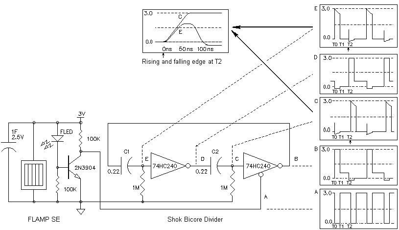
FLAMP SE
The Shok bicore in Figure 1, uses two inverters of a 74C240 chip with outputs controlled via the enable pin. The Shok bicore has output signals that toggle like a flip flop on the leading edge of the active low output enable signal. This is equivalent to dividing the frequency of the enable signal by a factor of 2. The only constraint for the basic prototype circuit is that the output enable pulse width must be shorter than the bicore period/2 or else more than one output pulse will be generated..
The signal to control the bicore enable line is generated by a simple FLED SE circuit. It uses a transistor to amplify the FLED current and generate a logic output signal. Every time the FLED fires, this active low signal enables the bicore outputs as shown in trace A. The FLED pulse has a fixed frequency but FLED trigger level depends on the level of ambient light falling on the FLED lens. To stabilize that trigger level use heat shrink tubing or black tape to cover the FLED.
The so-called FLAMP SE triggers at about 2.4V and continues to generate trigger pulses while the supply voltage is between 2.4V and 3.6V. This SE is normally used for solar applications using a 3V solar cell and a 0.47F -1.0F gold cap but those two components can also be replaced by a 3V battery for bench testing etc.
SHOK BICORE
The simple tristate enabled grounded bicore circuit in Figure 1 has output signals that change state like a flip flop, toggling high and low every time the enable signal goes active low. This Shok effect is easy observe and to reproduce but until now there was no theory available to explain this behavior.
Based on data acquired with a high speed oscilloscope, the timing traces are a good way to visualize what happens on the electronic level. These traces are idealized voltage waveforms at the Shok bicore enable input, the R/C input and output points. The waveforms together with some some validation experiments, will help make the theory behind the Shok effect become clear.
The Shok bicore circuit operation has two requirements: the circuit must have a way to memorize its current output state when the chip is disabled or powered down and it must toggle or invert that state when powered up or enabled. The Shok operation can be summarized as follows:
The last bicore state is memorized in the charges left on the timing capacitors when the circuit is tri-stated or powered down. When the bicore outputs are re-enabled, they enter a logic race to resolve the initial instability and now the differential timing capacitor charges help one output win this race with the new bicore state always opposite to the old state when the outputs were disabled.
The details of this operation are quite complex and are described
in several parts.
Figure 1
THE OUTPUT WAVEFORMS
The bicore outputs are successively enable and disabled with the low and high signals at the enable pin shown in trace A. The resulting voltage wavforms in traces B and D are unusual. When the outputs are enabled (T0), the output levels are 0V or 3V . But when the outputs are disabled (T1), these levels are no longer typical binary logic. Nor are they tristate logic levels in the conventional sense. They are in fact isolated analog voltage levels of the trapped charges in the timing capacitors when the outputs were disabled.
With the outputs disabled and isolated, these analog voltage levels at the output pins are sensitive to leakage current. Any loading of the output pins will discharge the analog voltage stored on the output pin side of the bicore capacitors that act as the memory elements. For example, adding 1M pull up resistors to the circuit in Fig 1 between the output pins and 3V completely destroys the Shok operation. Even measuring the outputs with scope probes can easily cause „loss of memory‰ and the duration of the disable signal must therefore be much shorter than the leakage time constant introduced by the measurement probes.
CMOS operational amplifiers were used as unity gain buffers for the purpose of measurement. To use the Shok bicore in practical application circuits, additional CMOS gates are used to buffer the outputs.
THE INPUT WAVEFORMS
The waveforms at the bicore inputs shown in trace C and E are also unusual in that when the enable signal in trace A is active low, they appear to be typical exponential voltage waveforms of the timing capacitors but when the outputs are disabled, the input voltage levels rapidly drop to 0V and thereby resetting the bicore to an „illegal‰ logic state prior to the next enable signal. This is an essential step in the memory and toggle sequence which will be discussed next.
SHOK MEMORY
How does the disabled bicore remember its last logic state? The answer is in the unusual analog output voltage levels shown in waveforms B and E.
To see how this charge is stored and how it causes the outputs to toggle we will walk through one complete „shoking‰ sequence. Note that for the sake of clarity, the term 0V will be used for voltage levels of 0V or less as the negative voltage levels here have no bearing on the Shok effect.
1. Let‚s assume that the enable signal (A) has just gone low (T0) and the bicore has assumed the normal metastable complimentary output state:
a. Enable (A) is 0V
b. Output (B) is 3V
c. Input (C) is at 0V.
d. Output (D) is 0V
e. Input (E) is 3V
The voltage across C1 is 0V but the voltage across R1 is 3V and the voltage at input E waveform starts to drop exponentially from 3V towards 0V as C1 charges up. Meanwhile the voltage on both side of C2 and across R2 is 0V and this charge on C2 remains virtually unchanged.
2. When the tristate signal goes high (T1) it isolates the bicore output pins. This disconnects one side of the C1 and C2 capacitor from the rest of the circuit and allows the voltage at the other side of the capacitors, at bicore input pins, to be instantly pulled down through R1 and R2 to 0V. At the same time, the voltage of the bicore output pins will follow the drop at the input pins with voltage across C1 (ie now with respect to 0V) equal to the voltage charged during the enabled time and corresponding to the exponential voltage drop on C1 shown in trace E at the end of the enable signal. The voltage on both sides of C2 remains unchanged near 0V. Note that both bicore inputs are at 0V just before the enable line in trace A goes active low again at T2.
SHOK TOGGLE
On the negative edge of the enable signal (T2), a signal race occurs when, as a result of the 0V level at the bicore inputs, both bicore outputs try to rise to 3V. This instability is resolved in a few nanoseconds as both P-channel mosfet output devices turn on thereby connecting the bicore outputs to 3V. As one side of the C1 and C2 are suddenly referenced towards 3V at the bicore outputs, the other side of C1 and C2 at the bicore inputs start to rapidly rise to a level equal to 3V minus any trapped charge.
The relatively slow 74C240 chip (compared to 74HC/AC240) was used in the prototype in order to make the fast rise time waveforms slow enough to be captured in detail with a storage oscilloscope as shown in the center trace in a closeup of the leading edge of input waveforms C and E superimposed at time T2 for ease of comparison.
It is the difference in the rate of rise of the voltage slope at the inverter inputs that determines which inverter wins the race to change state first. The slope is defined by dV/dT and dV is the size of the applied voltage step. That means that C2 with 0V residual charge will receive the largest voltage step on the input pin (trace C) and is therefore the first input level to cross the positive CMOS logic threshold. This causes the rising bicore output (trace B) to reverse and start back to 0V and this negative transition is capacitively coupled to input (E) reversing the voltage rise at that input so that it never crosses the logic threshold and therefore causes output (D) to continue on to 3V.
It was observed that when the difference in the slope is small, both bicore outputs may go low and oscillate for one cycle before the instability is resolved. This oscillation effectively double the difference and the outcome is the same: when bicore outputs B and D become stable they are active low and high respectively and this is the opposite to the output state after T0. The process repeats on every negative edge of the enable signal causing the outputs to alternate active high and active low.
If the enable signal is active low longer than the time it takes for the bicore to time out and assume the reverse state, several pulses will be generated at the bicore outputs but it is the last state before the bicore is disabled that is „remembered‰ and determines the state of the Shok bicore when re-enabled.
N/2 NEURONS
It is interesting to note that many gated oscillators can be used as flip flops to divide an enable signal by two as was described previously in the N/2 Neuron paper. By the gated oscillator method, the enable signal must be greater in duration than the oscillator period/2 but less than the oscillator period.. The tristated Shoke bicore toggles state on the leading edge of the enable signal. When the gating signal pulse duration is longer than the oscillator period, both basic circuits generate more than one output pulse for each enable pulse and hence the term N/2 with N being the duration of the enable pulse.
Despite some similarities, the respective toggling mechanisms are completely different and compared to the exotic operation of the Shok bicore, the logic of the gated oscillator divider will seem rather simple.
Next the Opto Shok Core and future applications of the Shok
architecture.