INTRODUCTION
The N/2 neuron is presented here as a proof of concept of a spiky stimuli
processing neuron! The N/2 neuron is so named because N/2 is represents
the ratio of 1/2*N output pulses for every input pulse.
The N/2 neuron has the capability to process spiky inputs and produce spiky outputs over a wide range of transfer functions that includes INHIBIT, ATTENUATE, REGENERATE and AMPLIFY. It seems intuitively obvious that networks of N/2 neurons would be capable of very complex stimuli processing. Despite of its complex capability, the N/2 neuron is a remarkable simple circuit.
THE N/2 NEURON MODEL
The neuron model of the N/2 neuron is the "programmable spike multiplier" . Input spikes are multiplied at the output by a factor N/2, programmed by the N/2 neuron internal process time constants. Programming (tuning) of the N/2 neuron is performed by adjusting analog variables which control two internal process time constants. The ratio of the two process durations determines the ratio of output to input spikes by a discrete factor of N/2 where N is a whole number equal to or greater than zero.
The electronic model for the N/2 neuron is the "gated oscillator with memory". An external negative transition is detected by the edge triggered Nv input generating an internal gating pulse which enables an internal oscillator to produce output pulses for the duration of the gating pulse. The last state of the oscillator output is retained when the gating pulse terminates. The number of pulses generated for each input pulse is determined by the ratio of the gating pulse width and oscillator period both of which are adjusted with analog (RC) components.
While the ratio of analog variable time constants is infinitely (continuously) variable, the ratio of input to output pulses is a discrete factor N/2. The first 4 factors of 0/2, 1/2, 2/2 and 3/2 are especially important since these generate 0, 1/2, 1 and >1 pulses for each input pulse.
The factor of N=0 (0/2) INHIBITS (blocks) the transfer of input pulses.
The factor of N=1 (1/2) ATTENUATES (divides) the transfer of input pulses by 2.
The factor of N=2 (2/2) REGENERATES (but delays) the transfer of input pulses by 1 ( 1 for 1).
The factor of N=3 and higher (3/2 and higher) AMPLIFIES the transfer of input pulses by N/2.
THE N/2 BINARY COUNTER
The N=1 factor is a special case with an interesting property: N/2 neurons you can count on! The N/2 "divide by 2" (or multiply by 1/2) transfer function is equivalent to a binary flip-flop and can be cascaded in a linear network to produce any length neuron ripple counters.
THE XOR N/2 NEURON
There are a number of N/2 neuron circuits which behave in similar ways. The XOR N/2 neuron consists of three series connected elements:
1. Nv input stage
2. XOR reversing stage
3. Oscillator output stage.
The XOR N/2 neuron combines an edge triggered input, a polarity control block, a Nu and a local +/- feedback loop. The RC components of the input and output stages are the analog variables that can be adjusted to give various time constants. It is the ratio of the Nv and Nu time constants that determine the transfer function of the N/2 neuron.
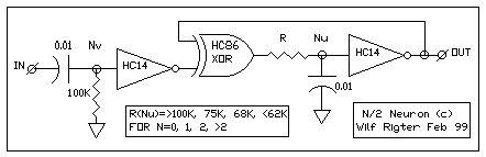
FIG 1 - THE XOR N/2 NEURON CIRCUIT)
As shown in FIG 1, The N/2 neuron external input uses a Nv at one input
of a XOR gate as a "edge triggered" Nervous neuron to generate a gating
pulse. The output of the XOR gate is connected to an Nu neuron and the
output of the Nu neuron is the external output of the N/2 Neuron. The second
XOR input is connected to the Nu output to provide positive or negative
feedback with the feedback polarity controlled by the Nv. Under stable
(no process) conditions the XOR provides positive feedback for the
Nu which then behaves as long term memory. When an input pulse occurs,
a Nv process is generated during which the XOR supplies negative feedback
to allow the Nu to cycle (Schmitt oscillator). Note the use of different
RC components for the Nv and Nu stages because the thresholds of HC86 and
HC14 are quite different which affects the time constant for the RC component
values. As with most Nv / Nu neuron circuits, the XOR N/2 neuron requires
tuning.
THE 2XOR N/2 CIRCUIT
A similar approach can be used with a gated CMOS oscillator normally
constructed with two inverters (see FIG 3). When the inverters are replaced
with non-inverting stages the circuit acts as a memory. The internal gating
pulse on the XOR inputs control whether the XORs are inverting or not.
It may be necessary to add a small (.001) capacitor to the OUTPUT to clean
up a glitch at the end of the Nv period because of slightly different thresholds
of the 2 XOR stages.
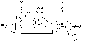
FIG 2 - THE 2XOR N/2 NEURON
The N/2 circuits in FIG 1 and FIG 2 use XOR gates, for which there
are no simple equivalents in biological systems and which are considered
to be too "digital" by some (apparently including Mark T.)
THE ELEMENTAL N/2 NEURON
The last N/2 neuron circuit is in that sense more biomorphic! It is designed with the simplest of all circuit elements avoiding all trappings of digital logic. The active components could in theory be reduced to the equivalent of 3 or 5 transistors. The ELEMENTAL N/2 NEURON consists of three series elements.
1. Nv input stage
2. Bilateral switch
3. Nv Oscillator
The ELEMENTAL N/2 NEURON uses two each resistors, capacitors, inverters and a single bilateral switch to form the gated oscillator/memory circuit. Since the input switching thresholds of these devices is symmetrical and near Vcc/2, the switching symmetry and time constants of the Nv input and the Nv oscillator stages are close in their characteristics and relatively stable with variations in Vcc. The other advantage of the ELEMENTAL N/2 NEURON is the reset of the capacitor charge when no process is active (Bilateral switch is closed). This means that every active process starts from zero capacitor charge which is precisely the same condition for a freerunning Nv oscillator at the start of each half cycle. As a result, the N/2 ratio pulse multiplying transfer functions of the N/2 change linearly with RC values and maintains a robust predictable relationship between the functions and component values and eliminates empirical "tuning"!
The ELEMENTAL N/2 NEURON circuit is shown in FIG 3.
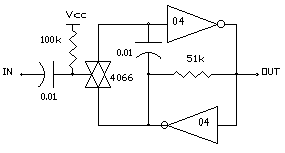
FIG 3 - THE ELEMENTAL N/2 NEURON
THE N/2 NEURON PROCESS
The examples of the two N/2 circuit in FIG 1 and 2 can be used to demonstrate the basic N/2 capabilities. The Nv generates an active low gating pulse at the input at each falling edge of the input waveform which enables the oscillator process and depending on the duration of the Nv input process (NvTC) and the oscillator process (XTC), the output will generate 0,1/2,1,1.5,2, etc output pulses for each negative input transition.
The XOR N/2 NEURON PROCESS
In the case of the XOR N/2 neuron, the gating pulse causes the oscillator output to input feedback to change from positive to negative feedback. An integrator followed by a Schmitt trigger with negative feedback is a classical Schmitt trigger oscillator alternately charging and discharging the oscillator capacitor with a period determined by the RC components and the Schmitt trigger input thresholds. Note that the initial oscillator process starts at 0V or Vcc and therefore has a much larger timeconstant than the subsequent processes which oscillate between the trigger thresholds. Depending on the ratio of the Nv and oscillator "process" time constants (NvTC and XTC), the oscillator produces 0, 1/2, 1 or more pulses for every negative input transition.
For example: An active low Nv process connected to one XOR input
changes the other XOR input to output polarity from inverting to non-inverting.
This changes the Nu output to input feedback from positive to negative
feedback and causes the voltage at Nu bias point will start to changing
in the direction of the Nu output polarity. Because of Nu input hysteresis,
there is a delay before the Nu bias point voltage reaches the trigger
threshold when the output changes state. If XTC is larger than NvTC,
the voltage at the Nu bias point will never reach this threshold before
the Nv pulse terminates and the transfer of input to output pulses is inhibited
(blocked) and the output remains unchanged (N=0). Longer NvTC periods permit
the bias point voltage to cross the threshold and the Schmitt trigger output
to reverse one or more times. This results in the various N/2 transfer
functions described in more detail
below.
The ELEMENTAL 2/N NEURON PROCESS
In the case of the ELEMENTAL N/2 neuron a negative transistion on the
NV input generates an active low gating pulse which turns off the bilateral
switch. This starts the Nv input time constant with zero charge on the
input capacitor which then charges up through the input resistor to Vcc.
During that time the bilateral switch is open and the Nv oscillator process
starts with zero charge on the oscillator capacitor (like the Nv input
capacitor) which charges towards 0V or Vcc depending on the state (memory)
of the last process. The processes of the Nv input and Nv oscillator are
very similar and if the switching thresholds are near Vcc/2 then these
two processes are symmetrical and effects of temperature and voltage variations
tend to cancel out.
INHIBIT
When the time constant of the Nv input (NvTC) is shorter than the time
constant for the first oscillator half cycle (XTC) then the oscillator
will return to it's starting state when the Nv process terminates and no
change in N/2 neuron output will result. As a result no input pulses
will reach the output so the N/2 neuron is said to be blocked or inhibited
(N=0)
ATTENUATE
If XTC is approximately equal to NvTC, the voltage at the oscillator bias point will just cross the threshold and oscillator output will change state. The inverted output then starts to charge the capacitor in the direction of the new output polarity. The oscillator output will not change until the bias point voltage reaches the second threshold. As long as the Nv gating pulse terminates before the second threshold is crossed, the oscillator output will only change state once. When the Nv pulse terminates positive feedback will hold the last oscillator output state (memory). On the next falling edge at the Nv input, the process repeats causing the oscillator/memory to change state (flip-flop) on each successive falling edge of the input waveform. As a result, half of the input pulses are transferred to the output (N=1). If several stages of N/2 (N=1) neurons, are connected in series, the resulting network behaves like a binary counter!
REGENERATE
If XTC is shorter than the NvTC, the voltage at the Nu bias point will
cross the first threshold, causing the oscillator output to change state
and then the charging voltage will reverse and the bias voltage will cross
the second threshold to change the oscillator output state once more. As
long as the Nv pulse terminates before the bias voltage again reaches the
first threshold, the oscillator output produces one output pulse for every
input pulse. (N=2)
AMPLIFY
If XTC is much larger than the NvTC, and the voltage at the oscillator input voltage crosses thresholds 3 or more times, the oscillator output will produce 1.5 or more pulses for every input transition.The transfer of input pulses is AMPLIFIED when more output pulses than input pulses are generated (N>2)
N/2 NEURON DEMONSTRATION
Unlike it's digital counterpart, the N/2 neuron depends on the ratio of the analog components for the Oscillator/Nv time constants to select a transfer function. In practice this means you can use a photodiode or other sensor to change one time constant and thereby successively change the transfer function of the N/2 Neuron from INHIBIT to ATTENUATE, REGENERATE and AMPLIFY.
To demonstrate the N/2 binary counter example (N=1), we can manually tune the time constants. Tuning the N/2 neuron for a specific function is simple. For example to tune the N/2 neuron for N=1 (divide by 2), apply a pulsing waveform (ie 2Hz MicroCore pulses) to the 2/N input pin. For the components shown, the active low input pulses must be >2ms and can be any frequency below 250 Hz. Higher frequencies can of course be achieved with different component values.
The 1M Nv pot is initially set for minimum and then slowly adjust the pot until you observe a squarewave at the output using a LED in series with a 5K resistor between the output and Vcc for indication. If the pot is adjusted further for smaller TC ratios, the N/2 neuron becomes a quantizing pulse multiplier, producing one output pulse for each input (N=2=REGENERATE) or 1.5, 2, 2.5, 3, etc output pulses for each input pulse (N>2=AMPLIFY). Note that the minimum input pulse width must always be greater than the Nv time constant. Also note that the fractional output pulses are a combination of a square wave and pulses which will also cause the LED to blink.
N/2 BIOMORPHIC CLOCK
After tuning the first N/2 neuron to divide by two, measure the resistance of the variable resistor and wire up the remaining gates (replacing the pot with fixed resistors) for a total of four N/2 neurons capable of counting 16 input pulses . Any number of N/2 (N=1) neurons can be cascaded to divide the input frequency by 2 to the nth power.
For example 5 chips (2 ea. H14 and 3 ea. HC86) provide a maximum of
12 neurons which will divide input pulses by 4096. I will design a simple
decoder which will reset an eleven stage counter chain clocked at one minute
intervals, when the counter reaches 1440 (the number of minutes in a day)
so that the dream of a "BIOMORPHIC CLOCK" is realized. Alternately 12 neurons
and decoders for 10, 6, 24 can be used to construct a BIOMORPHIC BCD CLOCK.
Remember that these are "ripple" counters and a 1ms delay (settling time)
is introduced at each stage. This limits the input frequency and/or
limits the maximum length of the network just like digital ripple counters
.
MONO N/2 NEURON
While the N/2 neuron circuit works fine in simple networks, there are some issues that need to be resolved, including normalizing the input and output pulse widths and pulse spacing required to stabilize the behaviour of N/2 neurons in complex networks. Narrow negative going input pulses will reset the input Nv before the gating pulse terminates and must be avoided. For a network of N/2(N=1) neurons this is not a an issue because the neuron output has a 50% duty cycle.
However in multiple input or complex N/2 networks a minimum pulse width
must to be guaranteed at both input and output to ensure predictable operation.
The input pulsewidth can be fixed by adding one more Bilateral switch at
the input stage as shown in MONO N/2 NEURON in FIG 4 . This switch
isolates the IN terminal from the Nv capacitor after the Nv is triggered
by an active low transition and for the duration of the NvTC uses R1 to
hold the IN side of the cap low. After the voltage across R2 is equal to
Vcc/2, the 4066 switch turns on to reconnect the IN to the cap after the
Nv times out. Resistor R1 provides a "low" impedance current path for charging
CNv while the IN terminal is isolated. The voltage drop across R1 introduces
a small error in the NvTC and the value of R2 should be at least 20 times
the value of R1 to minimize this error. Note the use of "elementary"
(non-digital) components for this non-retriggerable Nv monostable circuit.
I am presently exploring if an output pulse Nv is required for cascading
Amplifying N/2 stages.
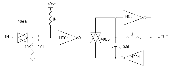
FIG 4 - THE ELEMENTAL MONO N/2 NEURON WITH FIXED GATING PULSE
COMPLEX N/2 NEURAL NETWORKS
I have not yet investigated complex N/2 neural networks that simulate spiky neuron biological systems although there would appear to be the potential for implementing processing functions using these simple N/2 networks. While not needed for N/2 in the N=0 to 2 modes, it appears that a network of AMPLIFYING (N>2) N/2 neurons require an output conditioning to generate fixed width output pulses.
The design objective is that one pulse cascading through several linearly connected (1 dimensional) stages of N/2 neurons in the AMPLIFY mode would produce a saturated pulse train with continuous equally spaced pulses of 2NvTC period. If the saturated pulse train encounters an N/2 neuron in the ATTENUATE mode the pulse train would be divided by 2. Several stages of attenuation will increase the interval between pulses and an INHIBIT mode neuron would block any pulses. In 2 dimensional networks of N/2 neurons in the AMPLIFY mode, a hemispheric wave of pulses would propagate from the single initiating pulse with the wavefront washing around groups of N/2 neurons in the ATTENUATE and INHIBIT mode.
NEURAL NETWORK SIMULATOR AND STATUS DISPLAY
I have just started to read about the Cellular Automata (CA) work of TOFFOLI. Several CA synthesizers programs (including JC) are available for the PC and are apparently in the public domain. These CA are like arrays of virtual BEAM machines (reproduction by any electronic means prohibited?) The process of each cell is determined by simple rules and the new states of the cell are calculated at each tick of the clock.
It may be possible to program the rule table for these CA programs to simulate N/2 neural networks. In any case an analog simulator would be very useful to test some of these ideas. I can't afford the specialized CA computing engines which are not the large scale arrays of silicon CA I had anticipated but instead seem to be RULE engines connected to memory planes with pipelines to video output. These CA engines like the CAM6 plug into a PC to generate 256x256 multicolor displays of CA using multi plane neighbor rule tables at ~60 frames/sec. ( I hope I got most of that right - anyone out there more familiar with the details?)
If a virtual MicroCore can be programmed into a PIC (which I'm sure it can be), it should be possible to write a program for the PC that simulates hundredsof photovore poppers, walkers, I wonder....