BEAM HEADS 101 - a beam circuit tutorial
Rev 1.1 11/99 - wilf rigter
WHAT'S A BEAM HEAD?
A BEAM HEAD is a mechanical and electronic assembly (Fig 1) that has the simple function of detecting and tracking a light source. It does this by rotating a set of photo sensors so that both receive an equal amount of light. The head is usually a circuit board containing the electronics mounted on the body of a small gear motor with the shaft of the motor, as the neck, attached to fixed support or mobile robot body. While seeking or tracking a light, a head continuously rotates around its neck. Since an umbilical power cord could lead to strangulation, the power source (battery or solar) is usually carried along with the electronics on the head.
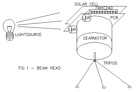
By adding a second motor and a duplicate set of electronics, the head may also look up or down. A head rotating in a 2D plane is referred to as a 2 Degrees of Freedom (2DOF) head and a head with the additional up down motion, scanning a 3D volume, is called a 3DOF head.
ELEMENTARY DESIGN DEAR WATSON
In any design, we combine elements from various older designs with new ideas to meet specific design requirements. The choice of one element may influence the choice of the other elements. For example, a large motor may require the addition of a separate motor driver. The PowerSmart head circuit is a simple solution to meet the design requirements for a small efficient 2DOF head controller. It has some unique design ingredients but it owes its concept and general form to Mark Tilden and others and ultimately to nature itself.
THE BASE
Of all the head elements, the base or support structure is the least sensitive to influencing the other head elements. It can be almost any shape that does not obscure "vision" and can made of any material sufficiently strong to hold up the head. Needless to say, for humans as well as robots, the overall aesthetics of the head are an important part of the design and while the simple tripod in this example will suffice, don't limit your imagination in your own design choices. It is also possible to wall or ceiling mount a head with the appropriate support. The details of a mobile base are beyond this introductory tutorial, but I hope to explore the design of a head mounted on a robot in a future article.
THE MOTOR
In the PowerSmart head design, an efficient 30 rpm gear motor was chosen but unmodified and modified hobby servos have also been used albeit with a different electronics design. Your choice of motors will have an influence on the design of the electronics and for now we will concentrate on small gear motors, typically found in video camera lens assemblies (ie Nihon - BGMicro), which can be driven directly from 74HC/AC logic. The motor I used was mounted with the shaft pointed vertically down. A small brass collar with a setscrew was attached to the end of the shaft and soldered to the copper wire tripod base.
THE BRAIN
The head has a brain made with various electronic components including resistors, capacitors, diodes, LEDs, solar cells, photo sensors, a voltage trigger and a single IC chip. The brain controls the motion of the head, in response to the location of a light spot within the field of vision. There are many ways to construct a head circuit: I used a Radio Shack 2"x2" square perfboard mounted with two stiff 1/4" wires connected to the solder terminals on the top of the motor body. The two photo diodes (PD) or light dependent resistors (LDR) inside small black tubes are mounted on one side of the board facing out, like a pair of eyes, in the same direction. To help you understand the basics before tackling what goes on in the brain of a HEAD, I have also included a short appendix with a simple description of electronic principles and useful mechanical models of electronic components used in this tutorial.
WHAT IS A POWER SMART HEAD
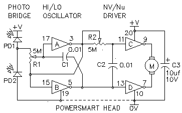
The POWERSMART (PS) head circuit was designed as an improved version of the bicore head. The operation of the PS head circuit will be described in more detail as an example of BEAM heads in general. The basic PS head schematic in Fig 2 contains everything except for the SE part. The PS head uses a 74HC240 Octal inverting buffer organized as 4 inverters in 2 groups each with a separate group output enable. If the second group of inverters is not yet used, they should have pins 1, 2, 4, 6 and 8 temporarily connected to 0V. Because of its power saving features the PS head is easily solarized but for some applications, the basic circuit plus batteries is all you need and of course there is another set of inverters in case you want to try building a 3DOF head. If want to solarize the head, one of the two the solar engines can be assembled and tested. The PS head is controlled with pin 19 connected to the SE enable output instead of 0V. The operation of the circuits is described in the next few sections following the order in which the PS head can be build and tested.
THE SOLAR ENGINE
The power supply for the SE head can be 3-6V Alkaline batteries but for long term autonomous operation power can be generated by a solar cell and stored in a large capacitor or nicad batteries as shown in Fig 3.
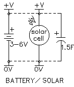
Fig 3
Both the bicore heads and PowerSmart heads can be solarized this way. The solar cell should be chosen to be compatible with the capacitor or rechargeable battery voltage rating. With sufficient light the solar cell will slowly charge the nicad battery or capacitor. A Ge diode is recommended placed in series with the solar cell to prevent the discharge of stored energy when the light level fluctuates. When the voltage of the stored charge is sufficient to operate the circuit the SE triggers. The output of the SE enables the head circuit and head will attempt to find and lock on to a bright light. For the PS design we look at two SE options: one using a MC34164 voltage supervisor in a simplified Chloroplast SE circuit and the other is a 1381 SE adaptation by Darrell Johnson shown also in Fig 10. Of course only one of the two SE circuits should be used.
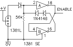
1381 SE
The 1381L voltage supervisor in Fig 4 is used to sense if the voltage on the power supply capacitor has sufficiently charged up (about 3V) and its output goes active high when the 1381 triggers. The 1381 has very small hysteresis and will quickly reset so its output is used to SET a latch made with two inverters of the second group. The inverted output of the latch provides and an ENABLE signal to hold the 74HC240 tri-state control pin19 active low. The latch is held SET by 2 diode in a positive feedback loop. When the supply voltage drops below the forward voltage of the 2 feedback diodes, the latch resets disabling pin 19. Because the PS head uses very little power when locked on, the charge on the solar cap can last a long time. When the motor runs, the voltage on the storage capacitor drops until it is less than the forward voltage of the 2 SE latch diodes at which point the latch resets. The voltage on Pin 19 will rise to V+, disabling the PS motion generator circuit and the power supply capacitor starts to charge up again from the solar cells.
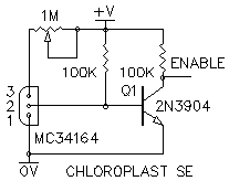
THE CHLOROPLAST SE
The Chloroplast SE (CSE) design in Fig 5 is much simpler and uses a MC34164 voltage trigger instead of a1381. No latch is required for the CSE since it cleverly uses a series input resistor to increase hysteresis between the set and reset voltages of the trigger. The 1M resistor is adjusted to set the trigger point and the reset occurs near 5V. Instead of the usual MPS12A darlington motor driver transistor in the original design by Craig Maniard, we use a 2N3904 for logic inversion to drive the 240 tri-state enable pin 19 active low. If you intend to build a 3DOF PS head, then both pin 1 and pin 19 would be enabled.
PS CIRCUIT DETAILS
In the next paragraphs, we describe each section of the PS head design as you build it. I recommend that you initially use a 3V to 6V battery or bench power supply to test and debug each step before proceeding to the next step. Even if you intend to build the solar version, you should build and debug the PS head circuit separately. Once the PS head circuit is set up, add the SE to solarize the circuit.
PS SENSORS
In Fig 6, we see a "photo bridge" with two light dependent resistors (LDR) or Photo Diodes (PD) used as the PS head "eyes". Either type of sensor is ok. Even green LEDs can be used instead of photo diodes but are inferior in terms of sensitivity and can only be used in bright conditions.
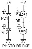
Fig 6
The photo bridge serves the same function as photo diodes used in bicore head circuits but unlike the bicore circuit, the photo bridge acts as a voltage divider with a midpoint "ratio-metric" output voltage which is largely independent of the absolute light level. When the top (turn right) LDR/PD is exposed to more light the midpoint voltage rises and when the bottom (turn left) LDR/PD is brighter then the voltage at the midpoint drops. So if both are exposed to the same light level the midpoint voltage is about 1/2V+. The LDR or PD pair should be carefully matched so that their resistance is approximately the same value when each is exposed to the same light level. Radio Shack currently sells a package of 5 LDRs for a few dollars but you may need to buy two packs to get good matched pairs. You can use a digital voltmeter connected between the midpoint of the photo-bridge and 0V to measure sensitivity. With both sensors pointing at a diffuse light source, the midpoint should at about 1/2V+. Don't worry if they are not perfectly matched, since this will only cause a error in the angle of the head when locked on to a light. One other supplier of LDRs and PDs is Solarbotics who sell premium matched pairs ready to use. Optional 1K resistors can be added to each leg of the photo bridge to provide a minimum resistance between +V and 0V to avoid excessive current flow if the LDR resistances decrease to very low values from exposure to very bright light. The important point to remember is that this part of the photo bridge produces an output voltage at the midpoint, which is proportional to the difference in light level on each sensor. That makes the circuit work over a large range of light levels with little change in sensitivity. The output voltage is used to control the duty cycle (on/off ratio) of the following oscillator stage in a very interesting and useful way.
PS HEAD HI/LO OSCILLATOR
The brain of the PS head is a classic CMOS astable oscillator with a difference: it has an additional input resistor, which provides control of the symmetry of the oscillator waveform proportional to the input voltage. This is a form of pulse width modulation over a range, which includes 0-100% on/off ratios. This is sometimes called a saturating oscillator since the output will be continuously high or low when the control voltage is higher or lower than the linear control voltage input range. The resulting circuit in Fig 7 is therefore called a High/Low Oscillator (HLO).
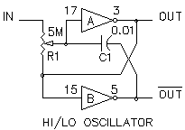
Fig 7
First let's examine how the HLO operates, without using the IN signal, behaving like a classic CMOS astable oscillator. The oscillator consists of 2 inverters with the input of inverter A serving as a summing node for several signals. As can be seen, a 5M potentiometer (R1) is connected from the output of inverter A back to it's own input. Because of the signal inversion, this is DC negative feedback, which tends to drive the input voltage of inverter A towards its 1/2V+ threshold. The output of inverter A is also directly connected to the input of inverter B. The output of inverter B is connected with a capacitor back to the input of inverter A. Because of the even (2) number of inverter in that feedback path, this is positive AC feedback, which drives the input to 0V or +V. This feedback capacitor (C1) has a similar function to the two capacitors in the bicore circuit described later. Assume inverter A with the input at 0V and the output at V+. So, initially, it has a voltage equal to V+ across the feedback resistor, which starts to discharge the voltage on the capacitor at the input of inverter A. When this input voltage eventually reaches the switch threshold of 1/2V+, it causes inverter A output voltage to rapidly drop from V+ towards the 1/2V. When the output of inverter A enters the linear threshold at 1/2V+ of inverter B input, the signal passes inverted through inverter B and its output starts to change. The output signal of inverter B, capacitively coupled back to the input of inverter A, will rapidly drive the changing input and output voltages to their saturated, supply voltage limited, high or low states. Once stable, these levels are again subject to dc negative feedback and the process repeats but in the reverse direction.
To recap, the voltage at inverter A output connected to the feedback resistor is opposite to the voltage on the capacitor at the summing input of inverter A, so the capacitor discharges through the resistor with the input voltage of A eventually reaching the threshold. This causes the output of inverters A and B to change and the capacitor sends the change back, in phase, to the summing input of inverter A thereby rapidly accelerating the change. When the outputs have changed state, the whole process repeats. The result is two square wave signals at the output pins of the inverters with one signal inverted with respect to the other. The frequency of the squarewave signal is inversely proportional to the product of the capacitor and resistor values. If you adjust the pot value to a smaller value the frequency increases. Before the final adjustments leave the pot in the center position
PULSE WIDTH MODULATION
As described in the photo bridge section, that circuit generates a voltage proportional to the difference in the left and right LDR light levels. Now we convert this voltage to a useful waveform to control the motor by connecting the photo bridge output to the IN terminal of the HLO as shown in Fig 8. While separate fixed resistors can be used, the adjustable potentiometers R1 and R2 are recommended for reduced parts count, to explore various head behaviors and to compensate for variations in voltage/logic thresholds
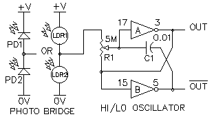
Fig 8
The potentiometer R1 is connected to pins 15 and 17 and the IN terminal to the midpoint of the photo-bridge to adjust the sensitivity, oscillator frequency and degree of pulse width modulation. Since the adjustment inherently affects all three functions, it requires tuning to give the right response. The output voltage of the photo-bridge is proportional to the difference of light on the photocells. That voltage is connected via part of R1 to the input of inverter where it is "summed" with the positive and negative feedback of the capacitor and the feedback resistor, which is the other part of the potentiometer. The photo-bridge difference voltage (Vp) results in an offset current which generates equal left and right pulse widths at the oscillator outputs when the Vp is balanced at 1/2V+ (or near the switching threshold) but changes the left right pulse width if Vp is unbalanced. It is useful at this point to also connect R2, C2, inverters C and D and the motor as shown in Fig 2 to observe the effects of the photo bridge and adjustment of R1 on the motor. For this part of the circuit testing, potentiometer R2 must be adjusted to zero ohms so that inverters C and D simply act as motor drivers. With R1 adjusted to the maximum value, and exactly equal light falling on the photo sensors, the motor receives equal duration left/right pulses, it vibrates rapidly but does not move. But when the photo-bridge is even slightly unbalanced, the effect of the offset current causes the pulse width to change asymmetrically producing a net rotation in the direction of the longer motor on time. By adjusting R1, the photo bridge sensitivity is changed and the motor will respond more slowly to light imbalance. As a rule, the value of R1 between inverter A input and output is adjusted between 90 - 50% of its full value before the sensitivity of the photo bridge becomes zero. Adjusting R1 to a smaller value yet is not recommended as it will only increase the frequency of the square wave, which will become audible but motion will drop to zero and the supply current will increase. As a small improvement, a 5M resistor can be added between the output of inverter A and R1. With R1 adjusted between 90 and 80%, the optimum (medium) sensitivity is achieved. At that point, the motor is stopped when the light is nearly balanced and the motor moves slowly left or right when the light is slightly unbalanced. When the photo-bridge is more unbalanced, the oscillator outputs are forced to a continuous high and low state and the motor rotates at full speed in the desired direction to balance the photo-bridge.
THE Nv/Nu OUTPUT STAGE
Let's have a look now at Fig 9, the Nv/Nu output stage. With the value of R2 reduced to 0 ohms during the adjustment procedure of R1, the two output inverters C and D have no effect on the complementary square waves at inputs IN and /IN other than inverting and isolating them from the motor load. If potentiometer R2 is 0 ohms and the photo-bridge output is balanced, the left right pulse width is symmetrical, and the head stops rotating but the power continues to flow through the motor while stopped and this is wasted energy. A solution to this problem is a circuit, which detects that condition and shuts off the power to the motor. . Increasing the R2 pot resistance value to mid point, it forms, in combination with C2 and inverter C, a "Nv/Nu" circuit. . The 0.02 cap shown in the schematic is recommended to increase the adjustment range and uses two 0.01 caps connected in parallel. When R2 is precisely adjusted, the Nv/Nu time constant will match the frequency of the HLO and when symmetrical or balanced as would be the case when the head is "locked on", the motor driver output voltages will be in phase, completely turning off the motor current and reducing supply current to about 2 ma.
When the photo bridge is slightly unbalanced, the HLO output waveforms are asymmetrical and the duration of either the left or right pulse widths will be longer than the Nv/Nu time constant and the motor will turn at a speed proportional to the difference. When the HLO output is high or low, those signals will of course quickly pass through the Nv/Nu circuit to drive the motor left or right at full speed.
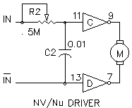
Fig 9
To recap: when the photo-bridge is greatly unbalanced, the HLO outputs are forced high or low. This results in a steady state condition in which the dc voltage from the two HLO outputs are can pass through the resistor but not the capacitor (in the fashion of a Nu). This results in the Nv/Nu stage having one driver on and one off and the motor continuously rotating towards the light source. Now assume that the light source is near the center of the field of vision and that the astable is oscillating but with a left pulse on time which is longer than the right pulse. Now the Nv/Nu stage acts like a Nv monostable but again with a small twist: unlike its cousin, the classic Nv, this one produces positive and negative output pulses. The result is that for the "right" direction pulses, the two outputs of the Nv/Nu stage are the same polarity and NO current flows through the motor. But for the "left" direction pulses, the Nv times out and for a short duration the two motor drivers have different output polarity. This provides a proportional output, which turns the head SLOWLY to the left. So when approaching the balanced condition the PS head slows down accordingly and the current also starts to drop off saving power. When the light on both photocells is fully balanced, the lowest power condition exists where the left and right pulses are the same duration and the Nv monostable never times out. Therefore the motor driver outputs always have the same polarity, no motor current flows and the motor is stopped. This is the low power (2ma) standby mode that gives the PS head its name. The circuit is now ready to hook up to the SE stage.
A SOLAR POWERSMART HEAD EXAMPLE
Fig 10 shows the solarized PS head layout drawing by Darrell Johnson using a 1381L solar engine.
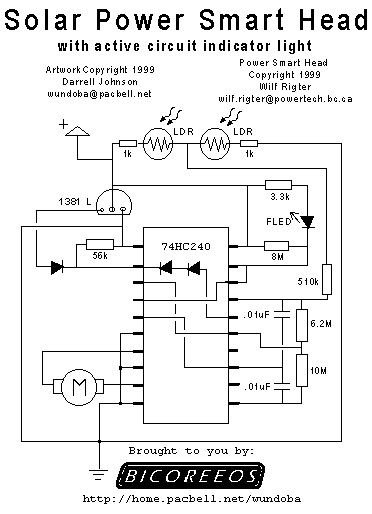
Fig 10
Note the unused input pins 6 and 8, which have been terminated to reduce power.
WHAT'S A BICORE HEAD
Most BEAM heads use the ubiquitous bicore circuit with photodiodes (Fig 10), designed by Mark Tilden, also used in walkers and photovores. The design is elegantly simple but has some shortcomings. One problem is the effect of the photo diodes on changing the bicore frequency as well as on/off time. Additional resistors can limit the influence of the PD's but this effectively limits operation to a narrow range of lighting conditions. The circuit also consumes a significant amount of power in proportion to the work of rotating the head and that's an important factor for battery or solar operation. There are reports of an updated bicore head design but at this time it has not been published.
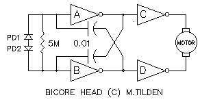
Fig 11
The bicore operation is as follows:
Assume that the voltage on bicore 240 inverter A input pin is V+ and that inverter B input pin is 0V. Therefore the difference voltage (V+) appears across the resistor and the reverse biased PD2. The output pin of inverter A will be opposite to its input voltage ie 0V and inverter B output pin will be V+. The current through the resistor and PDs starts to rapidly discharge the two capacitors with the voltage on both ends of the resistor changing towards 1/2V+. The rate of discharge is influenced by increased light level on PD2, which will effectively lower the total resistance. As the voltage across the resistor and PD2 drops the current decreases and the rate of discharge slows down. This is the characteristic exponential discharge curve for a RC network. Theoretically, if the switching threshold of the inverters (where the output start to change) was precisely 1/2V+ then it would take a long time for the caps to completely discharge. But unequal capacitor values, small threshold offsets, superimposed voltage ripple, thermal noise etc all contribute to cause the threshold to be crossed before the theoretical "end" of the discharge curve. When either inverter (ie inverter A) output voltage starts to change, that change is coupled through the capacitor to the input of inverter B. This voltage is added to the input voltage of inverter B pushing it across the threshold which in turn switches inverter B output voltage. Inverter B changing output voltage is coupled back through the capacitor to the input of inverter A and that pushes both inverter A and B input voltages rapidly to their respective 0V(-0.6V) and V+(+0.6V). The additional 0.6V is caused by the clamping action of the inverter input protection diodes. The inverter A and B output voltages will then be V+ and 0V respectively. Now the process repeats but with the capacitors discharging in the opposite direction and PD1 influencing the discharge rate in proportion to the light level. Photodiodes PD1 and PD2 therefore influence the on/off times of the bicore outputs causing it to rotate the head for a longer time in one direction compared to the other direction. When the PD light levels are balanced the head rapidly shakes back and forth equal distance effectively keeping it pointed in the same direction.